Placement
Placement is the step where the components of a circuit (standard cells in digital, or devices in analog) are arranged within the chip area.
A good placement ensures efficient routing, minimizes delay, and improves overall performance.
Why placement matters
- Directly affects timing, power, area, and routability.
- Influences routing congestion and manufacturability.
- For analog, placement is critical for matching, symmetry, and noise isolation.
Placement in digital design
Inputs:
- Floorplan (die/core dimensions, macros, IO positions).
- Gate-level netlist.
- Timing and congestion constraints.
Process:
- Standard cells are placed and legalized on predefined rows.
- Placement is optimized for wire length, delay, and congestion.
- Optional re-placement occurs after CTS or optimization.
- Density, utilization, and congestion are estimated to guide refinement.
Outputs:
- Placed DEF file.
- Reports for wire length, congestion, and timing impact.
Global, Legalization, and Detailed placement
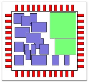
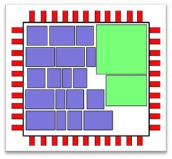
Placement is performed in multiple stages to gradually refine the position of all standard cells while ensuring design rules and timing are met.
- Global placement — generates an initial, coarse arrangement of cells to minimize total wire length and balance congestion.
- Cells may overlap at this stage.
- Uses analytical or force-directed algorithms.
- Provides a rough density and timing estimation.

Legalization — adjusts the preliminary positions to align cells to valid rows, remove overlaps, and respect placement blockages.
- Maintains minimal displacement from global placement results.
- Ensures cell orientation and row conformity.
- Creates a layout ready for detailed placement.
Detailed placement — performs fine adjustments to further optimize local wire length, timing, and routability.
- Includes cell swaps, shifts, and local reordering.
- May be repeated after CTS or optimization stages.

Additional Material: https://ocdcpro.github.io/educator-portal/material_browser.html?topic=digital&stage=placement
Placement in analog design
Focus:
- Device matching (current mirrors, differential pairs).
- Symmetry and common-centroid layouts.
- Minimizing parasitics and coupling.
Process:
- Manual arrangement of devices based on schematic intent.
- Placement is schematic-driven or constraint-assisted.
- Use of guard rings, dummy devices, and shielding.
Outputs:
- Layout drafts with critical device placement.
- Guidelines for later routing.
Mixed-signal considerations
- Isolation between noisy digital blocks and sensitive analog sections.
- Placement of decoupling capacitors and power domains.
- Ensuring short interconnects for analog critical paths.