Routing
Routing is the process of creating the physical interconnections between placed components inside a chip. After placement defines where each element sits, routing defines how signals, power, and clocks travel across metal layers. It connects all pins and terminals through patterned interconnects across multiple metal and via layers.
Why routing matters
- Determines signal integrity, timing, and power distribution.
- Affects chip area, congestion, and manufacturability.
- Must comply with all design rules (width, spacing, via limits) defined by the PDK.
- Errors in routing can cause shorts, opens, or parasitic effects that degrade performance.
Routing in digital design
Inputs:
- Placed DEF from placement step.
- Design rules from the PDK (minimum width, spacing, via rules).
- Timing constraints and power requirements.
- Routing guides generated by the global router.
- Blockages and keep-out regions inherited from the floorplan or macros.
Process:
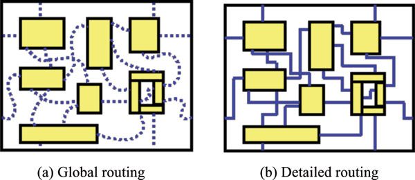
- Global routing — plans approximate paths for all nets to minimize congestion and estimate wire length.
- Track assignment — maps routes to specific metal tracks before final detailing.
- Detailed routing — finalizes exact wire geometries and via locations following all design rules.
- Post-route optimization — fixes violations, re-balances timing, and may perform ECO re-routing.
Outputs:
- Fully routed DEF and updated netlist.
- DRC-clean layout ready for sign-off or GDS export.
- Reports for DRC violations, wire length, congestion, and timing closure.
Global and Detailed Routing
Routing is typically divided into two main stages that progressively refine signal paths from abstract planning to final geometry.
Global routing — determines approximate routing paths between all pins and macros using coarse grid regions.
- Focuses on minimizing total wire length and congestion.
- Does not define exact metal tracks or vias yet.
- Generates routing guides that steer the detailed router.
Detailed routing — converts the global guides into exact physical wires and vias.
- Ensures compliance with all spacing, width, and via design rules.
- Assigns nets to specific metal layers and tracks.
- Performs DRC checking and incremental clean-up of shorts or opens.

Additional Material: https://ocdcpro.github.io/educator-portal/material_browser.html?topic=digital&stage=routing
Routing in analog design
Focus:
- Manual routing to ensure signal matching and symmetry.
- Shielding of sensitive nodes and differential pairs.
- Control of parasitic capacitance and resistance.
Process:
- Use of thick metal layers for power and high-current paths.
- Manual or assisted routing in layout tools (Magic, KLayout).
- Routing is guided by symmetry and matching constraints.
- Checking critical nets for length matching and noise coupling.
Outputs:
- Completed layout interconnects.
- DRC/LVS-clean layout ready for parasitic extraction.
Mixed-signal considerations
- Isolation between analog and digital routing domains.
- Use of guard rings and shielding to reduce substrate noise.
- Separate power domains and supply routing.
- Critical nets (e.g., reference voltages, clocks) should avoid crossing noisy digital regions.