Simulation
Simulation is the process of modeling the electrical or logical behavior of a circuit before fabrication.
It allows designers to validate functionality, performance, and timing under different conditions without building the physical chip.
Simulations can occur at multiple abstraction levels — from high-level logic to detailed transistor-level analysis — depending on the design stage and domain (digital or analog).
Why simulation matters
- Detects design errors early in the flow, before fabrication.
- Validates that circuits meet functional and performance specifications.
- Provides insight into timing, noise, and power behavior.
- Enables corner, Monte Carlo, and mixed-signal analysis.
Simulation bridges specifications and implementation, guiding iterative refinement throughout the design process.
Types of simulation
| Level | Description | Typical Tools |
|---|---|---|
| Behavioral / RTL | Logical verification of functionality using HDL (Verilog/VHDL). | Verilator, Icarus Verilog, GHDL |
| Gate-level | Timing-aware simulation of synthesized netlists. | Verilator, GTKWave |
| Transistor-level | Device-level analysis using circuit equations. | Ngspice, Xyce |
| Post-layout | Includes parasitics for realistic performance prediction. | Ngspice, Magic extraction, KLayout xRC |
| Mixed-signal | Co-simulation of analog and digital blocks together. | Ngspice + Verilator, Xyce + Icarus |
Digital simulation
Digital simulations verify that RTL code behaves as intended before synthesis.
They are fast, logic-based, and can run thousands of test vectors efficiently.
Process
- Write the RTL design (Verilog/VHDL).
- Create a testbench that applies inputs and monitors outputs.
- Run the simulation using tools like Verilator or Icarus Verilog.
- Visualize waveforms using Surfer or similar viewers.
Example — Simulating a Counter in System Verilog
// counter.sv
module counter(
    input clk,
    input rst,
    output reg [3:0] count
);
    reg [3:0] next_count;

    always @(*) begin
        next_count = count + 4'd1;
    end

    always @(posedge clk or posedge rst) begin
        if (rst)
            count <= 4'd0;
        else
            count <= next_count;
    end
endmodule// testbench.v
module testbench;
reg clk, rst;
wire [3:0] count;
counter DUT (.clk(clk), .rst(rst), .count(count ));
initial begin
$dumpfile("counter.vcd");
$dumpvars(0, testbench);
rst = 1;
#10;
rst = 0;
repeat (16) begin
clk = 1; #5; clk = 0; #5;
end
$finish;
end
endmoduleThis testbench toggles the clock and reset signals, recording all transitions to a .vcd file, which can then be inspected with Surfer to verify correct counting behavior.
 Simulation results
Additional Material: https://ocdcpro.github.io/educator-portal/material_browser.html?type=tutorial&topic=digital&stage=simulation
Analog simulation
Analog simulation focuses on continuous electrical behavior — voltage, current, gain, noise, and stability. It is based on solving nonlinear differential equations derived from the transistor models defined in the PDK.
Process
- Design the schematic in Xschem or a similar tool.
- Generate a SPICE netlist using the PDK device models.
- Run simulations using Ngspice or Xyce.
- Analyze waveforms and frequency responses in tools like plot, Bokeh, or Matplotlib.
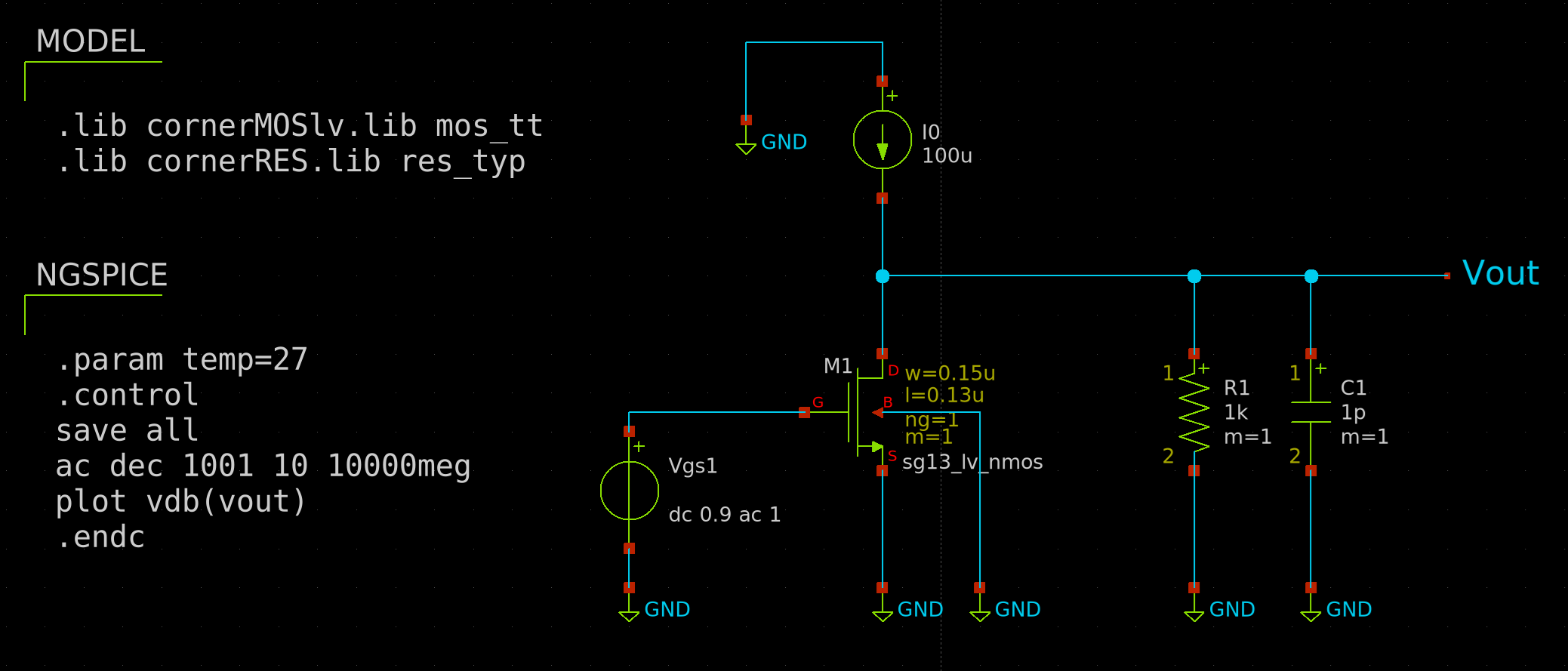
Example — Simulating a Common Source Amplifier
 Visualization of the synthesized netlist of the 4-bit full adder.
**.subckt cs
Vgs1 net1 GND dc 0.9 ac 1
XM1 Vout net1 GND GND sg13_lv_nmos w=0.15u l=0.13u ng=1 m=1
I0 GND Vout 100u
R1 Vout GND 1k m=1
C1 Vout GND 1p m=1
**** begin user architecture code

.lib cornerMOSlv.lib mos_tt
.lib cornerRES.lib res_typ

.param temp=27
.control
save all
ac dec 1001 10 10000meg
plot vdb(vout)
.endc

**** end user architecture code
**.ends
.GLOBAL GND
.end
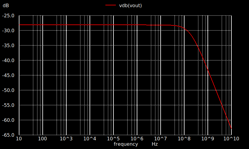
Visualization of the synthesized netlist of the 4-bit full adder.
This SPICE simulation models a simple NMOS amplifier. The output waveform shows how the transistor amplifies and inverts the input signal over time.
More information:
Ngspice Documentation
Xschem Tutorial – Analog Simulation
VSD – SPICE Simulation for Beginners (YouTube)
Post-layout and mixed-signal simulation
Once routing and parasitic extraction are complete, post-layout simulations verify that performance metrics (speed, gain, delay, etc.) remain within spec. These simulations include resistance (R) and capacitance (C) effects from the layout geometry.
- Digital post-layout: performed with timing back-annotation (SDF, SPEF).
- Analog post-layout: run on extracted SPICE netlists from Magic or KLayout.
- Mixed-signal: combines both, using co-simulation frameworks (e.g., Ngspice + Verilator).