Synthesis and Netlist Generation
Synthesis is the process of transforming a high-level circuit description into a lower-level representation that can be implemented physically.
In digital design, synthesis refers to mapping RTL code into a gate-level netlist using a technology library.
In analog design, there is no "logic synthesis," but netlists are extracted from schematics or layouts to represent the transistor-level circuit.
Why synthesis (or netlist generation) matters
- It connects the abstract design (RTL or schematic) to the physical design flow.
- It provides the first technology-dependent description of the design.
- It allows estimation of area, timing, and power before layout.
- It generates the reference netlist used for verification (LVS, STA).
Digital synthesis
Inputs:
- RTL description (Verilog, VHDL).
- Timing constraints (e.g., clock frequency, input/output delays).
- Target technology library (standard cells, Liberty files).
Process:
- High-level logic is transformed into Boolean networks.
- Optimizations are applied (area, power, timing trade-offs).
- Mapping is performed to available gates in the library.
Outputs:
- Gate-level netlist: list of standard cells and interconnections.
- Reports: area usage, timing analysis, power estimates.
Example — From RTL to Gate-Level Netlist
Below is a simple 4-bit full adder written in behavioral Verilog. This is the RTL-level description that a designer writes, focusing only on functionality — not the actual gates that will implement it.
module fulladd (  input [3:0] a,
                  input [3:0] b,
                  input c_in,
                  output c_out,
                  output [3:0] sum);

   assign {c_out, sum} = a + b + c_in;
endmodule
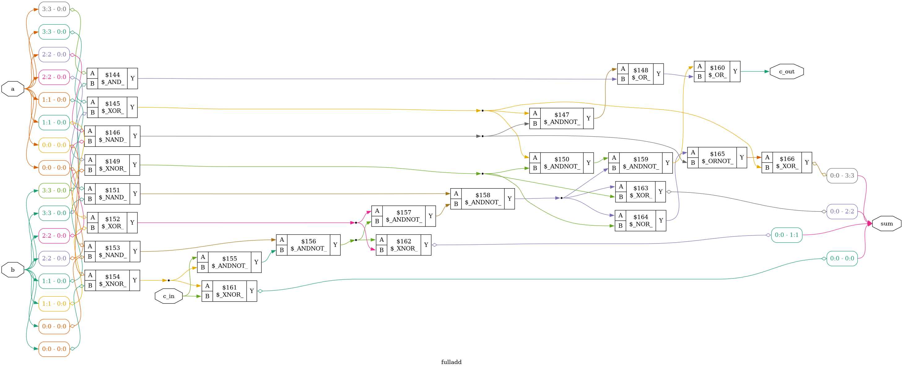
During synthesis, tools like Yosys translate this high-level description into a gate-level netlist, where all operations are expressed as logic gates (AND, OR, XOR, INV, etc.). Each intermediate wire and logic operation is explicitly listed.
module fulladd(a, b, c_in, c_out, sum);
  wire _00_;
  wire _01_;
  wire _02_;
  wire _03_;
  wire _04_;
  wire _05_;
  wire _06_;
  wire _07_;
  wire _08_;
  wire _09_;
  wire _10_;
  wire _11_;
  wire _12_;
  wire _13_;
  wire _14_;
  wire _15_;
  wire _16_;
  wire _17_;
  input [3:0] a;
  wire [3:0] a;
  input [3:0] b;
  wire [3:0] b;
  input c_in;
  wire c_in;
  output c_out;
  wire c_out;
  output [3:0] sum;
  wire [3:0] sum;
  assign _00_ = a[3] & b[3];
  assign _01_ = a[3] ^ b[3];
  assign _02_ = ~(a[2] & b[2]);
  assign _03_ = _01_ & ~(_02_);
  assign _04_ = _03_ | _00_;
  assign _05_ = ~(a[2] ^ b[2]);
  assign _06_ = _01_ & ~(_05_);
  assign _07_ = ~(a[1] & b[1]);
  assign _08_ = a[1] ^ b[1];
  assign _09_ = ~(a[0] & b[0]);
  assign _10_ = ~(a[0] ^ b[0]);
  assign _11_ = c_in & ~(_10_);
  assign _12_ = _09_ & ~(_11_);
  assign _13_ = _08_ & ~(_12_);
  assign _14_ = _07_ & ~(_13_);
  assign _15_ = _06_ & ~(_14_);
  assign c_out = _15_ | _04_;
  assign sum[0] = ~(_10_ ^ c_in);
  assign sum[1] = ~(_12_ ^ _08_);
  assign sum[2] = _14_ ^ _05_;
  assign _16_ = ~(_14_ | _05_);
  assign _17_ = _16_ | ~(_02_);
  assign sum[3] = _17_ ^ _01_;
endmodule
This representation is what is later used for placement, routing, and timing verification. Every connection is now technology-aware and can be mapped to physical standard cells.
 Visualization of the synthesized netlist of the 4-bit full adder.
Additional Material: https://ocdcpro.github.io/educator-portal/material_browser.html?topic=digital&stage=synthesis
Analog netlist extraction
Inputs:
- Schematic-level description (transistors, resistors, capacitors).
- Device models from the PDK.
Process:
- The schematic is translated into a SPICE netlist.
- Each component is mapped to a device model with parameters.
Outputs:
- SPICE netlist used for simulation.
- Extracted netlist later used for LVS comparison.
Example — OTA Netlist Extraction
Below we show a simplified Operational Transconductance Amplifier (OTA) schematic and its extracted SPICE netlist. The schematic (drawn in Xschem) defines transistor-level connections, while the extraction step produces the textual representation below.
 Schematic view of an OTA designed in Xschem.
Each line in the netlist corresponds to a transistor instance, defined by its terminals (drain, gate, source, bulk) and model type (from the PDK).
.subckt ota iref vin_n vin_p vdd vss vout
*.PININFO iref:I vin_n:I vin_p:I vdd:B vss:B vout:O
M1 net2 vin_n net1 vss sg13_lv_nmos w=15u l=2u ng=1 m=1
M2 net2 vin_p vout vss sg13_lv_nmos w=15u l=2u ng=1 m=1
M3 vout net1 vdd vdd sg13_lv_pmos w=2u l=1u ng=1 m=1
M4 net1 net1 vdd vdd sg13_lv_pmos w=2u l=1u ng=1 m=1
M5 vss iref net2 vss sg13_lv_nmos w=6u l=2u ng=1 m=1
M8 vss iref iref vss sg13_lv_nmos w=6u l=2u ng=1 m=1
.ends
This SPICE netlist is then used for electrical simulation (gain, bandwidth, noise, etc.) and for LVS comparison against the final layout to ensure consistency.
Mixed-Signal perspective
- Digital blocks → synthesized into gate-level netlists.
- Analog blocks → extracted into transistor-level SPICE netlists.
- Both netlists are integrated at the top level to form a complete mixed-signal system.
The mixed-signal integration step ensures correct pin naming, voltage domains, and timing alignment between the analog and digital domains.